Design of a High Gain Low Noise Amplifier at 3.3 GHz using CMOS Technology
Keywords:
Low noise amplifier, CMOS, 5G Communication, Inductor, Image RejectionAbstract
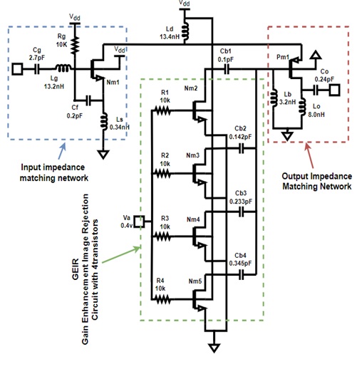
Low noise amplifier (LNA) is the important device used in field of communication. The main objective of this device is to boost the level of low power signal to a sufficient level without altering the signal to noise ratio in the circuit. This paper proposes a novel LNA with improved gain and optimized noise figure using Gain Enhancement and Image Rejection (GEIR) technique. CMOS technology is used in proposed work. LNA using CMOS at 90 nm technology is proposed using image rejection. The proposed amplifier boosts signal amplification using a 4 transistor CMOS GEIR network by providing proper input and output impedance matching. Simulations are performed using Cadence tool. The proposed amplifier is operating at a center frequency of 3.3 GHz and is able to achieve 14.5 dB gain and low noise figure. This could be useful in WIMAX application where high speed data rate at wide area coverage is required.
References
D. Wu, R. Huang, W. Wong, and Y. Wang, “A 0.4-V low noise amplifier using forward body bias technology for 5 GHz application,” IEEE Microw. Wireless Compon. Lett., vol. 17, no. 7, pp. 543 545, Jul. 2007.
C. Y. Cha and S. G. Lee, “A 5.2-GHz LNA in 0.35 m CMOS utilizing inter-stage series resonance and optimizing the substrate resistance,” IEEE J. Solid State Circuits, vol. 38, no. 4, pp. 669–672, Apr. 2003.
J. C. Bardin, "Cryogenic Low-Noise Amplifiers: Noise Performance and Power Dissipation," in IEEE Solid-State Circuits Magazine, vol. 13, no. 2, pp. 22-35, Spring 2021, doi: 10.1109/MSSC.2021.3072803.
N. Kumar and R. Bisht, "Design of an Ultra Low Power Low Noise Amplifier for 5-GHz band," 2020 IEEE International Conference for Innovation in Technology (INOCON), Bangluru, India, 2020, pp. 1-4, doi: 10.1109/INOCON50539.2020.9298326.
G. Feng, L. Zheng, Y. Wang and Q. Xue, "A 0.5-V 0.88-mW Low Noise Amplifier With Active and Passive Gm Enhancements in Sub-6 GHz Band," in IEEE Microwave and Wireless Technology Letters, vol. 33, no. 8, pp. 1159-1162, Aug. 2023, doi: 10.1109/LMWT.2023.3276915.
J. -T. Lim et al., "Bulk CMOS Low Noise Amplifier With Two Stage HPF Noise Matching Structure," in IEEE Transactions on Circuits and Systems II: Express Briefs, vol. 70, no. 6, pp. 1866-1870, June 2023, doi: 10.1109/TCSII.2022.3233537.
J. -Y. Hsieh and H. -C. Kuo, "A 0.4-V High-Gain Low-Noise Amplifier Using a Variable-Frequency Image-Rejection Technology," in IEEE Microwave and Wireless Components Letters, vol. 32, no. 4, pp. 324-326, April 2022, doi: 10.1109/LMWC.2021.3098249.
J. -Y. Hsieh and K. -Y. Lin, "A 0.6-V Low-Power Variable-Gain LNA in 0.18- $mu$ m CMOS Technology," in IEEE Transactions on Circuits and Systems II: Express Briefs, vol. 67, no. 1, pp. 23-26, Jan. 2020, doi: 10.1109/TCSII.2019.2902301.
B. Park, S. Choi, and S. Hong, “A low-noise amplifier with tunable interference rejection for 3.1-to 10.6-GHz UWB systems,” IEEE Microw. Wireless Compon. Lett., vol. 20, no. 1, pp. 40–42, Jan. 2010.
A. Sheldon and L. Belostotski, "A Cryo-CMOS Low- Noise Amplifier With 2.3-to-8.5-K Noise Temperature at 20 K for Highly Integrated Radio-Astronomy Receivers," in IEEE Microwave and Wireless Components Letters, vol. 32, no. 11, pp. 1319-1322, Nov. 2022, doi: 10.1109/LMWC.2022.3178579.
A. çağlar and M. B. Yelten, "A 180-nm X-Band Cryogenic CMOS LNA," in IEEE Microwave and Wireless Components Letters,vol.30,no.4,pp.395398,April2020,doi:10.1109/LMWC.2020.2979341
E.Cha et al., "0.3–14 and 16–28 GHz Wide-Bandwidth Cryogenic MMIC Low-Noise Amplifiers," in IEEE Transactions on Microwave Theory and Techniques ,vol. 66, no.11, pp.4860-4869, Nov.2018,doi:10.1109/TMTT.2018.2872566.
N. Yadav, A. Pandey and V. Nath, "Design of CMOS low noise amplifier for 1.57GHz," 2016 International Conference on Microelectronics, Computing and Communications (MicroCom), ,India,2016,pp.1-5,doi:10.1109/MicroCom.2016.7522438.
Low Noise Amplifier Design of CMOS Inductorless with Noise Cancellation Technique Mahesh Mudavath, K Hari Kishore, Sanjay Madupu, Prashanth Chittireddy , Srinivas Bhukya.
J. -F. Chang and Y. -S. Lin, "3–9-GHz CMOS LNA Using Body Floating and Self-Bias Technique for Sub-6-GHz 5G Communications," in IEEE Microwave and Wireless Components Letters, vol. 31, no. 6, pp. 608-611, June 2021, doi: 10.1109/LMWC.2021.3075279.

Downloads
Published
How to Cite
Issue
Section
License

This work is licensed under a Creative Commons Attribution-NonCommercial-NoDerivatives 4.0 International License.


